- 您现在的位置:买卖IC网 > Sheet目录490 > NTLJF4156NT1G (ON Semiconductor)MOSFET N-CH 30V 2.5A 6-WDFN
�� �
�
�NTLJF4156N�
�Power� MOSFET� and�
�Schottky� Diode�
�30� V,� 4.6� A,� m� Cool� ]� N?Channel,� with�
�2.0� A� Schottky� Barrier� Diode,� 2x2� mm�
�WDFN� Package�
�http://onsemi.com�
�Features�
�?� WDFN� Package� Provides� Exposed� Drain� Pad� for� Excellent� Thermal�
�V� (BR)DSS�
�MOSFET�
�R� DS(on)� MAX�
�I� D� MAX� (Note� 1)�
�?�
�?�
�?�
�?�
�?�
�Conduction�
�Co?Packaged� MOSFET� and� Schottky� For� Easy� Circuit� Layout�
�R� DS(on)� Rated� at� Low� V� GS(on)� Levels,� V� GS� =� 1.5� V�
�Low� Profile� (<� 0.8� mm)� for� Easy� Fit� in� Thin� Environments�
�Low� V� F� Schottky�
�This� is� a� Pb?Free� Device�
�30� V�
�70� m� W� @� 4.5� V�
�90� m� W� @� 2.5� V�
�125� m� W� @� 1.8� V�
�250� m� W� @� 1.5� V�
�SCHOTTKY� DIODE�
�4.6� A�
�Applications�
�?� DC?DC� Converters�
�?� Li?Ion� Battery� Applications� in� Cell� Phones,� PDA’s,� Media� Players�
�?� Color� Display� and� Camera� Flash� Regulators�
�V� R� MAX�
�30� V�
�D�
�V� F� TYP�
�0.47� V�
�A�
�I� F� MAX�
�2.0� A�
�MAXIMUM� RATINGS� (T� J� =� 25� °� C� unless� otherwise� noted)�
�Parameter�
�Drain?to?Source� Voltage�
�Symbol�
�V� DSS�
�Value�
�30�
�Unit�
�V�
�G�
�Gate?to?Source� Voltage�
�V� GS�
�±� 8.0�
�V�
�S�
�K�
�Continuous� Drain�
�Current� (Note� 1)�
�Steady�
�State�
�T� J� =� 25� °� C�
�T� J� =� 85� °� C�
�I� D�
�3.7�
�2.7�
�A�
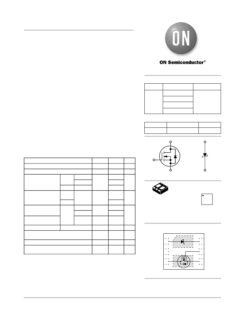
�N?CHANNEL� MOSFET�
�SCHOTTKY� DIODE�
�MARKING�
�t� ≤� 5s�
�T� J� =� 25� °� C�
�4.6�
�DIAGRAM�
�G�
�Power� Dissipation�
�(Note� 1)�
�Steady�
�State�
�t� ≤� 5s�
�T� J� =� 25� °� C�
�P� D�
�1.5�
�2.3�
�W�
�1�
�WDFN6�
�CASE� 506AN�
�1� 6�
�2� JLM� G� 5�
�3� 4�
�Continuous� Drain�
�Current� (Note� 2)�
�Power� Dissipation�
�(Note� 2)�
�Steady�
�State�
�T� J� =� 25� °� C�
�T� J� =� 85� °� C�
�T� J� =� 25� °� C�
�I� D�
�P� D�
�2.5�
�1.8�
�0.71�
�A�
�JL� =� Specific� Device� Code�
�M� =� Date� Code�
�G� =� Pb?Free� Package�
�(Note:� Microdot� may� be� in� either� location)�
�Pulsed� Drain� Current�
�t� p� =� 10� m� s�
�I� DM�
�20�
�A�
�PIN� CONNECTIONS�
�Operating� Junction� and� Storage� Temperature�
�T� J� ,� T� STG�
�?55� to�
�°� C�
�Source� Current� (Body� Diode)� (Note� 2)�
�Lead� Temperature� for� Soldering� Purposes�
�(1/8� ″� from� case� for� 10� s)�
�I� S�
�T� L�
�150�
�2.4�
�260�
�A�
�°� C�
�A�
�N/C�
�1�
�2�
�K�
�6�
�5�
�K�
�G�
�Maximum� ratings� are� those� values� beyond� which� device� damage� can� occur.�
�Maximum� ratings� applied� to� the� device� are� individual� stress� limit� values� (not�
�normal� operating� conditions)� and� are� not� valid� simultaneously.� If� these� limits� are�
�D�
�3�
�D�
�4�
�S�
�exceeded,� device� functional� operation� is� not� implied,� damage� may� occur� and�
�reliability� may� be� affected.�
�1.� Surface� Mounted� on� FR4� Board� using� 1� in� sq� pad� size� (Cu� area� =� 1.127� in� sq�
�[1� oz]� including� traces).�
�2.� Surface� Mounted� on� FR4� Board� using� the� minimum� recommended� pad� size�
�of� 30� mm� 2� ,� 2� oz.� Cu.�
�(Top� View)�
�ORDERING� INFORMATION�
�See� detailed� ordering� and� shipping� information� in� the� package�
�dimensions� section� on� page� 7� of� this� data� sheet.�
�?� Semiconductor� Components� Industries,� LLC,� 2006�
�June,� 2006� ?� Rev.� 4�
�1�
�Publication� Order� Number:�
�NTLJF4156N/D�
�发布紧急采购,3分钟左右您将得到回复。
相关PDF资料
NTLJS1102PTBG
MOSFET P-CH 8V 3.7A 6-WDFN
NTLJS2103PTAG
MOSFET P-CH 12V 3.5A 6-WDFN
NTLJS3113PTAG
MOSFET P-CH 20V 3.5A 6-WDFN
NTLJS3180PZTBG
MOSFET P-CH 20V 3.5A 6-WDFN
NTLJS4114NT1G
MOSFET N-CH 30V 3.6A 6-WDFN
NTLJS4149PTBG
MOSFET P-CH 30V 4.6A SGL 6WDFN
NTLJS4159NT1G
MOSFET N-CH 30V 3.6A 6-WFDN
NTLTD7900ZR2G
MOSFET PWR N-CHAN 9A 20V 8MICRO
相关代理商/技术参数
NTLJF4156NTAG
功能描述:MOSFET NFET 2X2 30V 4A 70MOHM RoHS:否 制造商:STMicroelectronics 晶体管极性:N-Channel 汲极/源极击穿电压:650 V 闸/源击穿电压:25 V 漏极连续电流:130 A 电阻汲极/源极 RDS(导通):0.014 Ohms 配置:Single 最大工作温度: 安装风格:Through Hole 封装 / 箱体:Max247 封装:Tube
NTLJS1102P
制造商:ONSEMI 制造商全称:ON Semiconductor 功能描述:Power MOSFET −8 V, −8.1 A, COOL Single P−Channel, 2x2 mm, WDFN package
NTLJS1102PTAG
功能描述:MOSFET PFET WDFN6 8V 8.1A 36mOhm RoHS:否 制造商:STMicroelectronics 晶体管极性:N-Channel 汲极/源极击穿电压:650 V 闸/源击穿电压:25 V 漏极连续电流:130 A 电阻汲极/源极 RDS(导通):0.014 Ohms 配置:Single 最大工作温度: 安装风格:Through Hole 封装 / 箱体:Max247 封装:Tube
NTLJS1102PTBG
功能描述:MOSFET PFET WDFN6 8V 8.1A 36mOhm RoHS:否 制造商:STMicroelectronics 晶体管极性:N-Channel 汲极/源极击穿电压:650 V 闸/源击穿电压:25 V 漏极连续电流:130 A 电阻汲极/源极 RDS(导通):0.014 Ohms 配置:Single 最大工作温度: 安装风格:Through Hole 封装 / 箱体:Max247 封装:Tube
NTLJS2103P
制造商:ONSEMI 制造商全称:ON Semiconductor 功能描述:Power MOSFET
NTLJS2103PTAG
功能描述:MOSFET PFET WDFN6 12V 5.9A 0.025 RoHS:否 制造商:STMicroelectronics 晶体管极性:N-Channel 汲极/源极击穿电压:650 V 闸/源击穿电压:25 V 漏极连续电流:130 A 电阻汲极/源极 RDS(导通):0.014 Ohms 配置:Single 最大工作温度: 安装风格:Through Hole 封装 / 箱体:Max247 封装:Tube
NTLJS2103PTBG
功能描述:MOSFET PFET WDFN6 12V 5.9A 0.025 RoHS:否 制造商:STMicroelectronics 晶体管极性:N-Channel 汲极/源极击穿电压:650 V 闸/源击穿电压:25 V 漏极连续电流:130 A 电阻汲极/源极 RDS(导通):0.014 Ohms 配置:Single 最大工作温度: 安装风格:Through Hole 封装 / 箱体:Max247 封装:Tube
NTLJS3113P
制造商:ONSEMI 制造商全称:ON Semiconductor 功能描述:Power MOSFET −20 V, −7.7 A, uCool TM Single 2x2 mm, WDFN Package